Influence of Nitrogen and Vapour Phase Soldering on the Formation of Tombstone Effect
In the surface assembly process of electronic products, especially in the high-volume reflow soldering process, the tombstone effect of passive chip components to the PCBA assembly soldering adds a lot of trouble. With the SMC / CMD micro/miniaturisation, reflow soldering of these chip components will appear upright, this phenomenon is also known as the Manhattan effect.
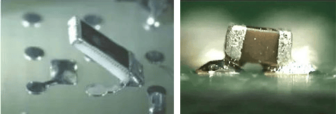
Figure 1. Tombstone phenomenon
This phenomenon occurs mainly in small chip components, they are soldered on the opposite poles of the surface mount pads, in the soldering process, the components stand up vertically, as shown in the figure. Sometimes it is partially upright, and sometimes the component is completely upright on a pad, like a tombstone in a cemetery.
With the miniaturisation and lightweighting of chip components and the application of high-temperature lead-free solders, the effect of tombstone defects has become more significant. Tombstoning effects tend to occur in gas-phase reflow and nitrogen reflow systems, and even when using new batches of components and PCBs.
Tombstone effect due to initial wetting differences
aspcms.cnOne of the causes of the tombstone effect is the difference in the initial wetting force of the solder on the two ends of the passive component, which results from the difference in the wetting force of the surfaces of the two solder ends and the surface tension of the solder. If one solder end is reflowed and wetted more quickly than the other, the forces acting on that end to form a solder joint may cause the other solder end of the component to lift, creating the tombstone phenomenon.
The wetting mechanism consists of three important parameters: initial wetting time, wetting force and complete wetting time. Complete wetting occurs when the maximum force is applied to the solder joint and the component, so the difference in complete wetting time is directly related to the generation of tombstone defects.
Effects of Nitrogen and Vapour Phase Soldering
The effect of nitrogen and gas phase soldering on tombstone effects is significant. During reflow welding, nitrogen prevents surface re-oxidation and accelerates the onset of initial wetting; the rate of temperature rise in gas phase welding should be controlled, and like the nitrogen environment, the gas phase of gas phase welding prevents surface re-oxidation. Under both process conditions, the component to be welded has a much reduced oxidation of the metallised surface as it enters the reflow zone, allowing faster wetting. If the reflow soldering temperature rises too quickly at this point, or if the direction, speed and temperature of the airflow are not uniform, then the SMD component is more likely to be pulled up, creating a tombstone effect.
The faster initial wetting does not provide enough time to reduce the ΔTS, and the additional delay in the initial wetting time to reduce the ΔTS is exactly what is necessary to reduce the occurrence of tombstone defects. Therefore, while we see the obvious benefits of nitrogen and gas phase welding, we need to take extra precautions to minimise the occurrence of tombstoning.
Measures to avoid the tombstone effect
1. Adjust the reflow temperature curve, increase the preheating temperature and preheating time to reduce the temperature difference between the two ends of the component;
2. The use of nitrogen protection reflow soldering, to control the amount of residual oxygen in the nitrogen environment, preferably 500ppm;
3. Under the premise of ensuring the strength of the solder joint, the pad size should be as small as possible, because after the pad size is reduced, the amount of solder paste applied is reduced accordingly, and the surface tension of the solder paste melting is also reduced. The heat capacity of the entire pad is reduced, the probability of melting solder paste on both pads at the same time greatly increased.
Fitech Solder Paste
Fitech is a leading global manufacturer of soldering materials for microelectronics and semiconductors, providing customers with solder paste with the right melting point and performance. Please feel free to call us for more information.
Application of Micro-Sized Cu in Power Devices
The application of power device products has expanded to a considerable number of industries, such as automotive, aerospace, and military industries. Power devices need to be able to adapt to higher operating temperatures (>250°C), which significantly increases the demand for equipment materials. Transient liquid phase (TLP) bonding is considered a reliable technique for preparing high-temperature solder joints, which allows soldering at relatively low temperatures while generating higher soldering remelting temperatures. However, TLP bonding takes a long time to completely consume low melting point metals and requires several hours of annealing to form stable solder joints.
1. Micro-sized Cu particles
Liu et al. deposited Sn layers on Cu particles. The average diameter of Cu particles is 6.2μm. The average thickness of Sn coating was about 0.5μm. The Cu particles were then made into a paste consisting of 85wt% particles and 15wt% terpene alcohol solvent. The Cu-Cu solder joint with slurry was preheated in the air at 130°C for 3 mins to evaporate the solvent. The solder joint was continuously heated to 300°C and remained 30s. The heating rate was 1°C/s. The entire process was carried out using a hot press bonding system under an external pressure of 10MPa. A formic acid atmosphere was introduced to reduce the oxide layer on the Sn coating and Cu substrate.
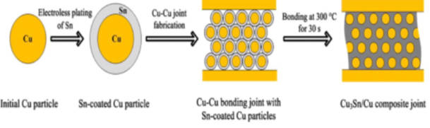
Figure 1. Transient Liquid Phase Sintering (TLPS) Bonding Process.
2. Experimental results
During the TLPS bonding process, Cu6Sn5 IMC is formed at the beginning of the solder joint. As the temperature rises above 210℃, the Sn plating layer of Cu particles gradually melts. As the temperature continues to rise, Sn begins to consume significantly, the number of Cu3Sn begins to increase, and Cu6Sn5 gradually decreases until it disappears completely after heating to 300℃. In high-temperature application environments, solder joints generally do not contain thermally unstable Cu6Sn5 phases. When the composition of the solder joint is located in the Cu-rich region of the Cu-Sn system, Cu6Sn5 tends to transform into Cu3Sn.
As shown in Figure 2, the atomic ratio of Cu to Sn is 3:1 in the gray area of the bonding solder joint. The black particles uniformly distributed in the gray area are Cu particles, indicating that the Cu3Sn IMC phase in the bonding solder joint contains uniformly distributed Cu particles. After aging at 300°C for 200h, the microstructure characteristics of the two-phase mixture are almost consistent with the structure after soldering, indicating that the thermodynamics of the solder joint remains basically stable at this temperature. Importantly, due to the similar microstructures before and after soldering, the strength of the solder joint varies slightly with increasing aging time.
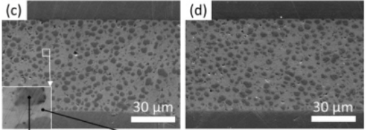
Figure 2. The SEM image of TLPS solder joints. (c) after heating at 300 ℃ for 60s (d) after aging at 300℃ for 200h.
3. Fitech's solder paste
In addition to TLPS bonding, traditional lead-free solder paste can still be used for the soldering of power devices. Shenzhen Fitech has professional experience in the research and production of high-temperature solder paste, which can provide customers with high-quality gold-tin solder paste for high-temperature welding needs. Fitech's gold-tin solder paste has the advantages of stable viscosity, low residue, and high solder joint strength. Welcomes customers to cooperate with us in depth.
4. Reference
Liu, X.D., He, S.L. & Nishikawa, H. (2016). Thermally stable Cu3Sn/Cu composite joint for high-temperature power device. Scripta Materialia, vol.110, pp.101-104.